
Your MEMS
Manufacturing Partner
At Rogue Valley Microdevices, we don’t just build your MEMS device. We work with you from concept to commercialization to make sure it’s fool-proof. From thin film processes to ready-to-ship wafers, we have you covered.
Our Services


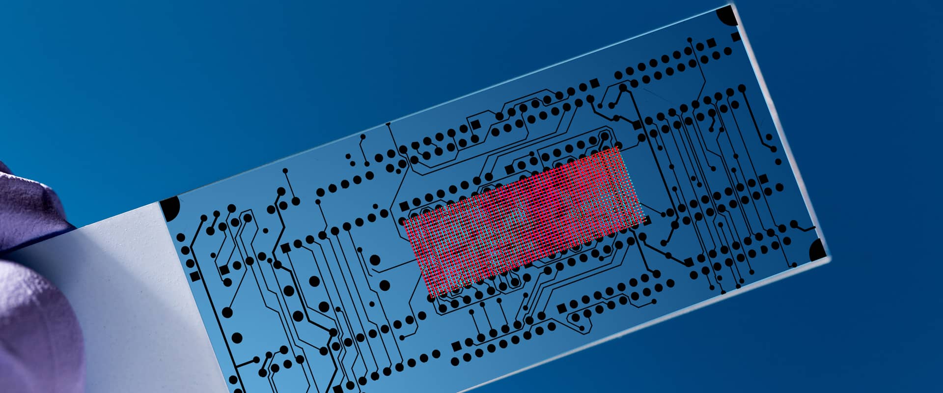
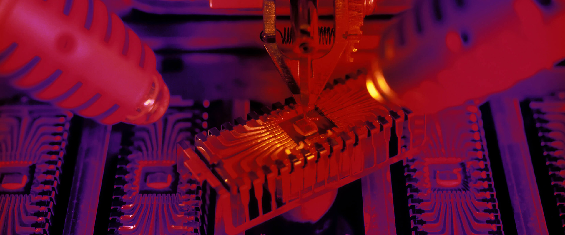
MEMS Foundry

Thin Films
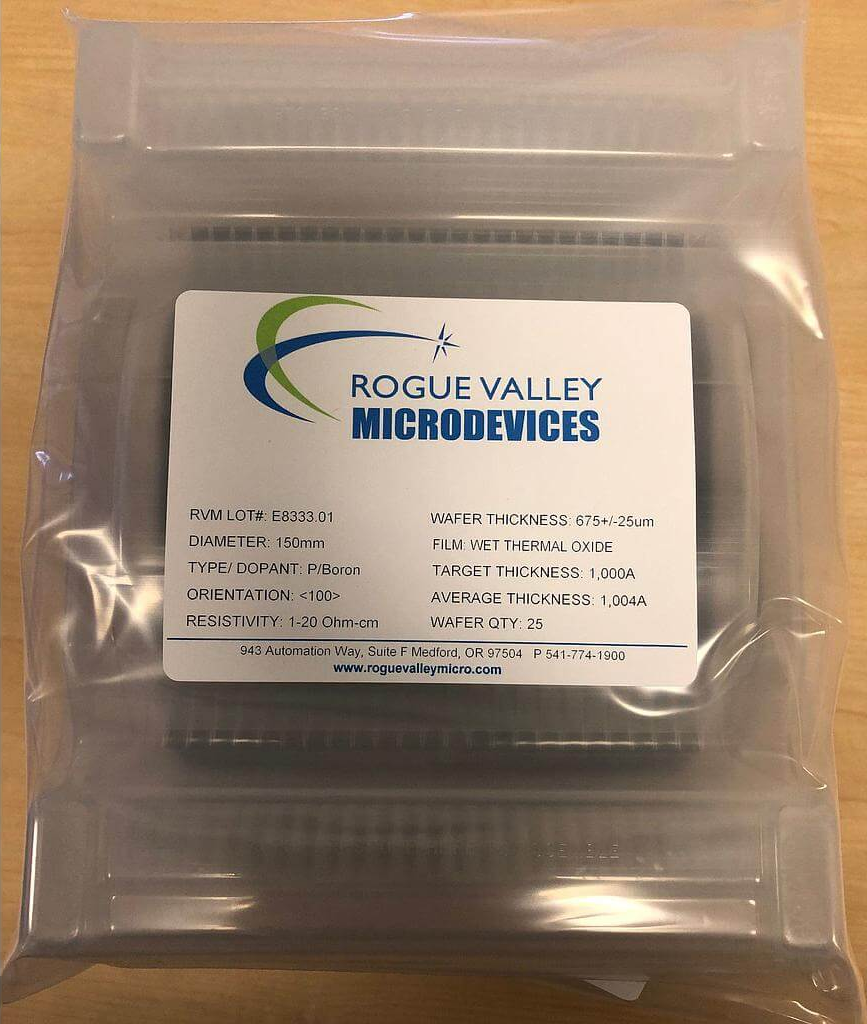

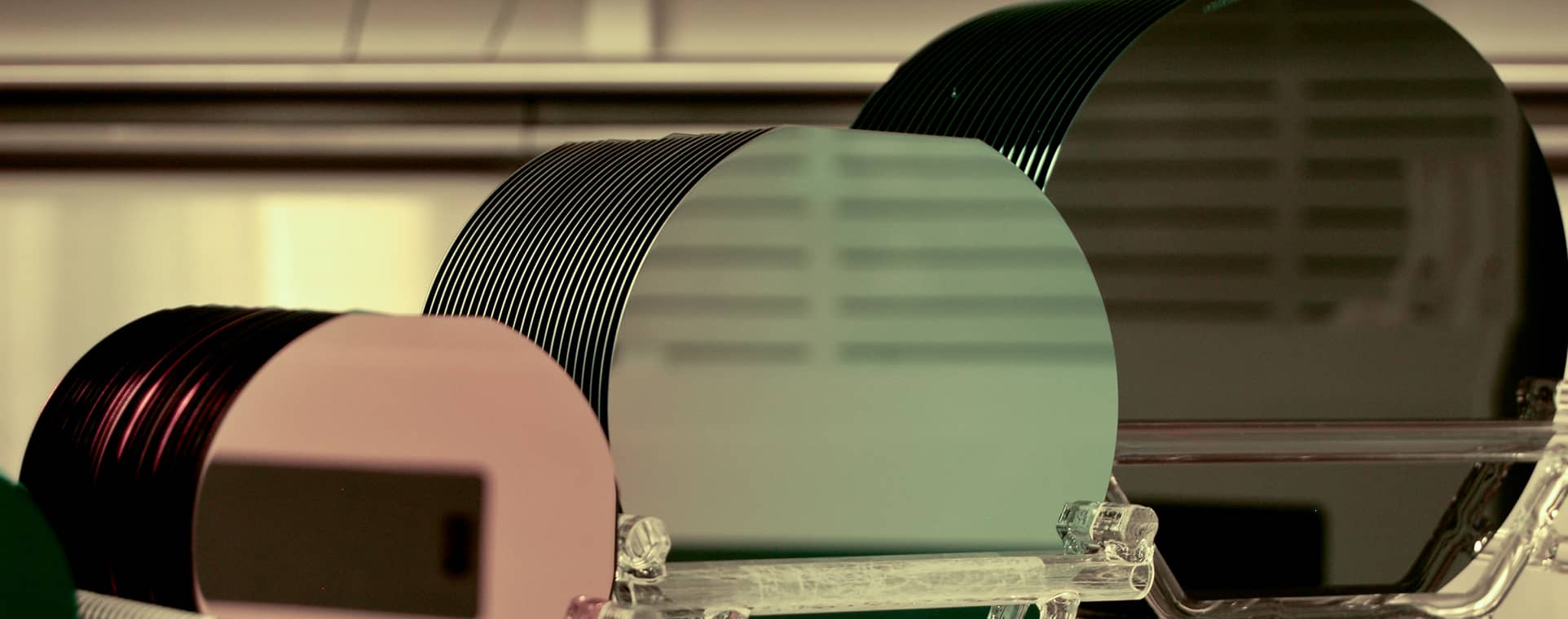
In-stock Wafers

Careers
We’re hiring! Become part of our team.
What could be better than an exciting career helping to build the next cool product? Getting to do it with fun people in a beautiful location. Let’s explore how we can change the world—and your experience in it—by welcoming you to an innovative company in the exciting microelectronics industry.
Ready To Get Started?
The Latest
Oregon-based Rogue Valley Microdevices to Open Microfabrication Facility in Palm Bay
– Company’s second pureplay MEMS fab creates 75 new high-tech jobs along Florida’s Space Coast MEDFORD, Ore.—June 28, 2023—Rogue Valley Microdevices, an Oregon-based advanced manufacturing company specializing in microelectromechanical systems (MEMS)—tiny intelligent devices that improve our quality of life in […] Read More »
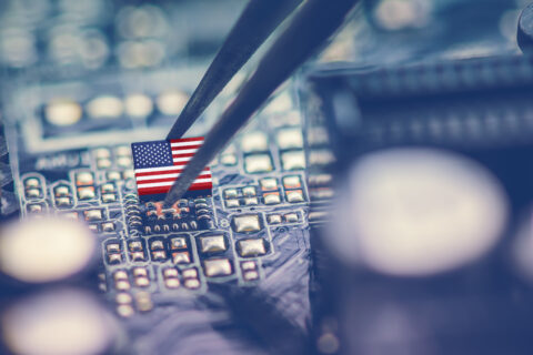
What Do Small Companies Need to Know about the CHIPS Act?
IBM’s Poughkeepsie, N.Y. site was the backdrop a few weeks ago for one of President Biden’s speeches promoting the passage of the $52B CHIPS (Creating Helpful Incentives to Produce Semiconductors) and Science Act, a rare piece of legislation for which […] Read More »
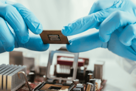
State of Semiconductor Industry 2021
By Dilek Isik Akcakaya, PhD Microelectronics manufacturing is heavily dependent on the availability of semi-grade Silicon and technologies that enable precise patterning of or on the Silicon Wafers. Creating nano- and micro-scale stationary and/or moving structures allows advancements in computers, […] Read More »